

Analog Devices大電流電感 AD8553儀表放大器的獨特架構降低并聯設備噪聲。
Analog Devices AD8553自調零儀表放大器具有獨特架構,其兩個增益設置電阻沒有公共結點(參考文獻1)。IC的前端是一個精密電壓電流轉換器,其中一個增益設置電阻R1設置跨導的大小。IC的末端是一個精密電流電壓轉換器,它的反饋電阻R2的值,根據G=2(R2/R1)共同決定全部電壓增益。可以發現,兩個增益設置電阻是獨立的,輸入端的電壓控制電流源,用減少放大器數量的方法,滿足嚴格的低噪聲要求。
多使用放大器減小噪聲分兩步。首先,假設放大器的隨機噪聲源相互獨立。進一步,假設噪聲服從高斯分布。當平均經典電壓放大器的輸出時,通過使用N個放大器和三倍電阻減少噪聲到1/ (參考文獻2)。AD8553內部架構對幾乎無限個并聯IC工作時,僅允許使用N+1個電阻。通過并聯更多IC各自的輸入引腳,連接內部電壓電流源容易并聯工作(圖1)。微伏級的輸入電壓偏置與若干IC的并聯輸入引腳配合不當是無害的,因為電壓電流轉換器的輸出電阻理論上是無窮大的。
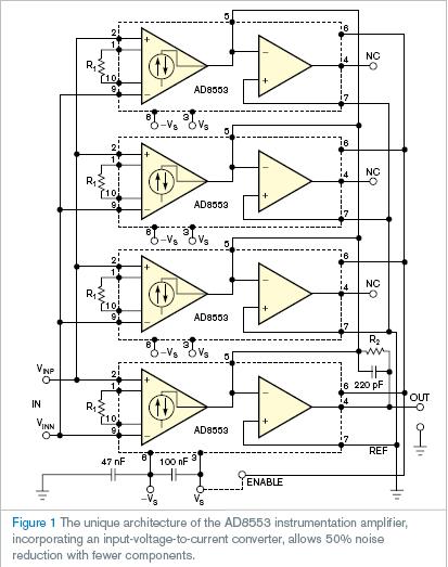
并聯N次輸入端的網絡結果是單IC輸出電流的N(VINP–VINN)/(2R1)或N倍。可以僅使用N個IC電流電壓端的一個。端反饋電阻為R2/N,在此,R2為單IC的期望電壓增益AV值。由于放大器噪聲的主要來源為輸入端,假設N個并聯電壓電流轉換器輸出電流的隨機器件標準差為σNI=σI×![]() ,σI為電壓電流轉換器輸出電流的隨機器件標準差。這些結果與參考文獻2中的不同,文獻中作者通過多電壓平均的方法實現減小噪聲。另一方面,圖1電壓電流轉換器的共模輸出中電流的決定成分為單IC的N倍。下面的公式計算RSNR(相對信噪比),定義超過輸出噪聲標準差的輸出電流:RSNRN=(N×I)/(σI×
,σI為電壓電流轉換器輸出電流的隨機器件標準差。這些結果與參考文獻2中的不同,文獻中作者通過多電壓平均的方法實現減小噪聲。另一方面,圖1電壓電流轉換器的共模輸出中電流的決定成分為單IC的N倍。下面的公式計算RSNR(相對信噪比),定義超過輸出噪聲標準差的輸出電流:RSNRN=(N×I)/(σI×![]() )=
)=![]() ×RSNR1。實際上,意味著電路噪聲減少到單IC的1/
×RSNR1。實際上,意味著電路噪聲減少到單IC的1/ ![]() 。
。
英文原文:
Autozeroed amplifier with halved扁平型電感 noise needs few components
The unique architecture of the Analog Devices AD8553 instrumentation amplifier permits paralleling devices to lower noise.
Marián Štofka, Slovak University of Technology, Bratislava, Slovakia; Edited by Charles H Small and Fran Granville -- EDN, 10/25/2007
The Analog Devices AD8553 autozeroed instrumentation amplifier has a unique architecture in that its two gain-setting resistors have no common jun差模電感器ction (Reference 1). The first stage of the IC is a precise voltage-to-current converter, in which the first gain-setting resistor, R1, sets the magnitude of the transconductance. The end stage of the IC is a precise current-to-voltage converter, in which the value of its feedback resistor, R2, co-determines the overall voltage gain as G="2"(R2/R1). You can exploit the fact that the two gain-setting resistors are separate and that the input stage is a voltage-controlled current source to lower the component count in amplifiers wi一體成型電感器th extreme noise-reduction demands.
You can use more amplifiers to reduce noise in two ways. First, assume that the sources of random noise in the amplifiers are mutually independent. Further, assume that the noise obeys a gaussian distribution. When averaging the outputs of classic voltage amplifiers, you can reduce the noise to a fraction of 1/ by using N amplifiers and three times as many resistors (Reference 2). The internal structure of the AD8553 allows you to use just N+1 resistors for an almost-unlimited number of ICs operating in parallel. By paralleling the respective input pins of more ICs, the connected internal voltage-to-current sources easily operate in parallel (Figure 1). The microvolt-range inpu電感電流t-voltage-offset mismatch at paralleled input pins of several ICs is harmless here because the output resistances of the voltage-to-current converters are theoretically infinite. 大功率電感廠家 |大電流電感工廠